A semiconductor diode is a unidirectional electronic device. It allows current flow in one direction only. This has a nonlinear voltage to current relationship.
B. Schematic Symbol
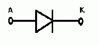
Figure 2.1 A Diode
The diode has two operations. The forward biased operation , where it allows current flow and the reverse biased operation, where it does not allows current flow. Ideally, it operates like a switch. It is either ON or OFF. It has two terminals, the Anode (A) and Cathode (K).
C. The Ideal Diode
The ideal diode has a zero resistance to current flow if forward biased, and has an infinite resistance to current flow if reversed biased. It is either an ON or OFF single pole single throw switch.
D. The vD versus ID plot of an Ideal Diode
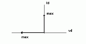
Figure 2.2. The vD vs. ID plot of an Ideal Diode
In figure 2.2, it is shown that the plot coincides with the positive y axis and the negative x axis. The y-axis is the current axis and the x-axis is the voltage axis. Since at forward biased the ideal diode offers a zero resistance, the plot at the y-axis shows this operation, where the voltage across it is zero and the current through it is maximum. The plot that coincides at the negative x-axis shows the ideal diode reverse biased operation, where, the current that passes through it is zero and the voltage across it is maximum. In this operation the ideal diode offers an infinite resistance.
Return
Return to Top
A practical diode has a forward resistance at the order of hundred ohms or less and a reverse resistance at a thousand's ohm or more. In this diode the potential barrier in the PN junction takes a major role in its operation. This potential barrier is technically termed as the threshold voltage (VTH) and is equal to 0.7v for a silicon diode and 0.2v for germanium diode. Thus the resistance of the diode in both operations is due to this barrier in the junction. Figure 2.3 shows the basic construction of the diode with this potential barrier.
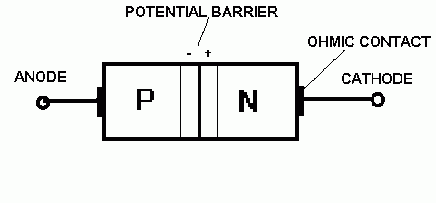
Figure 2.3. The Potential Barrier of the Diode
A. The vd-Id curve of a Practical Diode
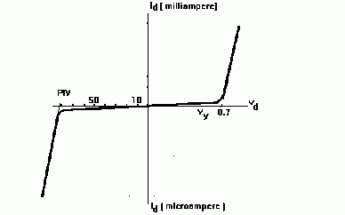
Figure 2.4. The vD-ID Curve of a Practical Diode
Figure 2.4 shows that the real diode operation is in the first and third quadrant of a Cartesian plane. In the first quadrant the forward biased operation falls, and the reverse biased operation in the 3rd quadrant. In the forward biased region, the plot shows that there is no appreciable flow of current below the threshold voltage. As vd is increased above vTH diode current starts to flow appreciably in nonlinear way. The manufacturer gives the maximum forward current limit. If the diode is driven above this limit heat is uncontrollably generated in the junction. This is known as thermal runaway. If not controlled abruptly the device will burn out. The only opposition to the flow of this forward current is the resistances offered by the P and N regions known as the diode bulk resistance with a typical value of 1 to 25 ohms and junction resistance.
In the reverse biased region of the diode operation, the plot shows that points below the PIV or breakdown point, current is at its minimum level at the order of microamperes. Notice also that the voltages below this point are at the order of ten to hundreds of volts. Thus in these points of operation the diode exhibits a very high resistance. The reverse current flowing in these points of operation is known as the leakage current and is negligible if the diode is operated in room temperature. Above the normal operating temperature, the diode operating current must be derated or adjusted below normal so as to accommodate the effect of this leakage current which value or amount increases as temperature in the junction increases.
Once the applied reverse voltage exceeds the Peak Inverse Voltage, the maximum reverse voltage that the diode can handle usually given by the manufacturer, the leakage current will increase exponentially in uncontrolled manner to the destruction of the device. Thus for safety purpose the applied peak voltage to the diode must be lesser than the specified PIV of it.
B. Typical Ratings of a PN Diode
- Maximum average forward current is given at 250C and refers to the maximum average current the diode can handle safely without structural damage.
- Peak recurrent forward current is in the form of repetitive pulses and is the maximum amount of such that can be applied to the diode in forward direction.
- Maximum surge current is the max. non-repetitive current that the diode can withstand at a few second. Diode will be damage if current equal this value will stays longer.
- Peak Inverse Voltage ( PIV ) - the maximum reverse bias voltage that can be applied to the diode before breakdown.
- Reverse recovery time ( trr ) - the time spent by the diode from the ON state to fully OFF state.
- Junction Capacitance- total capacitance offered by the junction during forward and reverse biased operation.
C. The Rectifier Diode
The rectifier diode is a PN junction diode. It is mainly used for rectification. Figure 2.5 is a basic nomenclature of a rectifier diode.
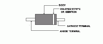
Figure 2.5 Common Rectifier Diode Nomenclature
Return
References:
- Malvino, Albert Paul: Electronic Principles, 5th Ed.; Glencoe Division of Mcmillan/ McGraw-Hill School Publishing Company, USA, 1993.
- Matthews,, John I.: Solid-State Electronics Concepts; McGraw-Hill, Inc., N.Y., USA 1972.
- Millman, Jacob & Grabel Arvin: Microelectronics, 2nd Ed.; McGraw-Hill Book Company, Singapore, 1984.
- Schuler, Charles A. : Electronic Principles and Applications, 3rd Ed.; McGraw-Hill Book Company, Singapore, 1989.
- William, Gerald E.: Practical Transistor Circuit Design and Analysis; McGraw-Hill Book Inc., USA, 1973.
Review Question:
- How the diode threshold voltage affects its operation?
- What is the resistance of a PN junction diode below breakdown point in reverse biased operation?
- What is PIV?
- What are the two important electrical parameters of a PN junction diode? describe each.
- What identifies the cathode terminal in a real diode? Give two specific answer.
- Describe the operation of an ideal diode.
Return to Top
Return to Electronics Principle Web Index